STMicroelectronics and Metalenz Partner to Transform Optical Sensing for Consumer, Automotive, and Industrial Applications
- Agreement encompasses development of manufacturing processes, industrialization of meta-surface optics, and technology licensing
- Revolutionary flat-lens technology brings performance, power, size, and cost advantages to complex optical systems
Stay tuned
To receive frequent updates via email, subscribe to our press releases.
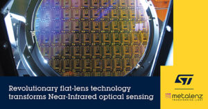
 STMicroelectronics (NYSE: STM), a global semiconductor leader serving customers across the spectrum of electronics applications, and Metalenz Inc., the pioneer in meta-surface design and commercialization, today announced a co-development and license agreement that will see ST develop manufacturing processes for Metalenz’s meta-optics technology for next-generation smartphones, consumer devices, healthcare, and automotive applications. Metalenz is a spin-out of the group of Federico Capasso at Harvard University, where the technology was invented. This breakthrough technology is expected to be ready for mass production by the end of this year.
Metalenz’s multifunctional meta-surface optics enable new forms of sensing for the next generation of smartphones and other consumer devices, as well as healthcare and automotive applications. For example a camera built around this new flat-lens technology can collect more light for brighter images and produce images of the same or better quality than traditional refractive lenses while consuming less power and taking up less space.
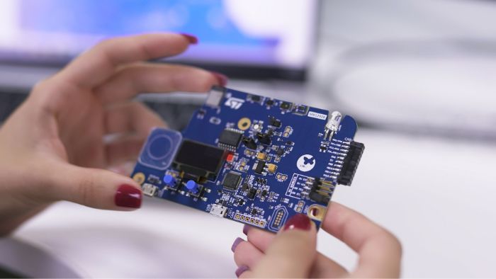
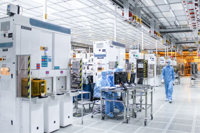
ST will integrate Metalenz’s meta-surface optics technology into ST’s existing diffractive optics manufacturing process at its 300mm wafer fab in Crolles, France, leveraging ST’s position at the forefront of the fast-growing Near-Infrared (NIR) optical sensing market. Today ST leads the market for time-of-flight (ToF) proximity and distance sensors with over 1 billion devices shipped to customers.
Eric Aussedat, Executive Vice President & General Manager of ST’s Imaging Division, said, “With its advantages in power, efficiency, and performance, multifunctional optics technology can be a game changer for the next generation of optical sensors used in smartphones and other consumer devices, as well as healthcare and automotive applications. In combining Metalenz’s advances with our proprietary technology, manufactured in our state-of-the-art 300mm production facility in Crolles, this partnership will support ST’s continued offering of the most innovative and advanced optical-sensing solutions to its customers.”
“We are thrilled to be working with an industry leader like ST. The technology developed by Metalenz is a perfect complement to ST’s advanced capabilities and market position,” said Dr. Rob Devlin, CEO and co-founder of Metalenz. “We adopted a fabless business model so that we can focus on the innovation and design of revolutionary optics to transform sensing from smartphones to automobiles. Working with ST enables us to expand our product offering while leveraging ST’s high-volume fabrication capability and enables ST’s already differentiated product lines to reach new heights with Metalenz inside.”
Note to editors
The technology used in today’s smartphones is changing and developing at a very fast rate to squeeze more and better functionality into less space. Still, the lenses remain essentially unchanged since medieval times. That’s now changing, with meta-surface optics introducing a new breed of lens, which works on very different fundamental principles. Instead of using bulkier curved surfaces, meta-surface optics combine multiple complex optical functions in a single flat layer. This shrinks the size of each lens element while also cutting the number of lens elements needed, dramatically reducing the size of the optical lens, the number of components, the complexity of assembly, and the overall cost.
The technology developed by Metalenz is a perfect complement to ST’s advanced capabilities. Combining semiconductor manufacturing and optics, ST will use advanced lithographic masks to build tunable diffractive-wavefront layers on a meta-surface in a semiconductor wafer fab. Like silicon ICs, the flat meta-surface lenses are processed in a semiconductor clean room using the same manufacturing technology. The lenses will feature nanostructures one-thousandth the width of a human hair. These nanostructures appropriately bend light rays to realize in a single layer the same functionality as a complex multi-element refractive lens system.
This technology is initially targeted at the fast-growing NIR market. NIR wavelengths are used in all the 3D sensing functions, such as face identification, autofocus assist, mini-LIDAR, and AR/VR depth mapping, that are becoming standard in today’s smartphone. Given the benefits, optical lenses made in a semiconductor wafer fab could someday be as common as traditional refractive lenses.
About STMicroelectronics
At ST, we are 46,000 creators and makers of semiconductor technologies mastering the semiconductor supply chain with state-of-the-art manufacturing facilities. An independent device manufacturer, we work with more than 100,000 customers and thousands of partners to design and build products, solutions, and ecosystems that address their challenges and opportunities, and the need to support a more sustainable world. Our technologies enable smarter mobility, more efficient power and energy management, and the wide-scale deployment of the Internet of Things and 5G technology. Further information can be found at www.st.com.
![]() About Metalenz
About Metalenz
Metalenz, founded in 2016, is the first company to commercialize meta-optics. Our meta-surface technology provides complex, multifunctional optical performance in a single semiconductor layer and enables moving large-scale production of optics into semiconductor foundries—printing lenses like computer chips. As a fabless semiconductor company, Metalenz is focused on the design and unique applications of meta-optics, transforming sensing across consumer, healthcare, and automotive applications.
The company has the exclusive worldwide license to the portfolio of foundational intellectual property relating to metasurfaces developed in the Capasso Lab at Harvard University and has more than 20 patents on innovations that simplify and improve optical devices across multiple markets. For more information, please visit https://www.metalenz.com/
For Press Information Contact:
Michael Markowitz
Director Technical Media Relations
STMicroelectronics
Tel: +1 781 591 0354
Email: michael.markowitz@st.com
Carlos Calvo
VP of Product
Metalenz
Tel: +1 (857) 301-8510
Email: carlos@metalenz.com
Stay tuned
To receive frequent updates via email, subscribe to our press releases.


