STMicroelectronics has presented a strategic project to create a new R&D Digital Twin center that will take shape at the company’s Castelletto site in Lombardy, west of Milan. The initiative aims to strengthen advanced research and development activities, accelerate innovation across the company, and pave the way for product and technology solutions that were previously out of reach.
 By Fabio Gualandris, President, Quality, Manufacturing, and Technology
The creation of this new R&D Digital Twin Center in Castelletto, Italy marks an important step in transforming how we conduct semiconductor research and development, including how quickly we do so.
The targeted benefits of this new approach are practical and measurable: shorter technology-development cycles, faster time-to-market, stronger first-pass success, higher engineering productivity, lower development costs and greater confidence before physical validation. Ultimately, these capabilities should help ST bring differentiated technologies and products to customers faster and with greater predictability.
This ambition responds to a fundamental challenge facing the semiconductor industry. Technologies are becoming more complex, development costs are rising and the required time to market continues to shrink. Yet today, much of the learning process at the heart of R&D still depends on physical silicon. Differences between models and measured results and the late discovery of reliability, layout or process interactions can lead to additional development loops, consuming time, engineering resources and investment.
Our goal is to move from physical iteration toward digital anticipation.
To support this transition, the new center will connect physics-based modelling, simulation, data, artificial intelligence, engineering knowledge and silicon feedback in one integrated R&D environment. It will support technology development, process and device modelling, layout and design, reliability, qualification and testing.
The objective is not to replace physical experimentation. Silicon validation will remain essential. Instead, we want to explore more possibilities digitally, identify potential issues earlier and reach physical validation with greater confidence. This can reduce repeated learning loops and accelerate the readiness of new technologies.
For customers, this means a stronger foundation for differentiated technologies, improved predictability, faster time-to-market and more scalable innovation across product families.
At the core of this approach is the digital twin: a continuously evolving digital representation of the interactions between semiconductor processes, devices and designs. It is calibrated using data from physical experiments and silicon characterization. Each experiment improves the digital models, helping subsequent development become faster, more accurate and more predictive.
This feedback loop is especially powerful within ST’s integrated device manufacturer model. Our capabilities across technology R&D, product design, manufacturing and testing allow knowledge to circulate across engineering disciplines. Connecting these capabilities digitally can help teams make better-informed decisions earlier and apply learning across technologies, products and system-level solutions.
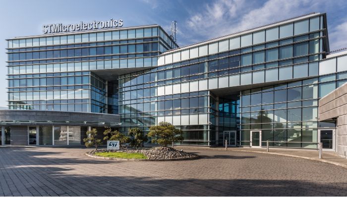
Castelletto was chosen because it already brings together many of the capabilities the new R&D Digital Twin Center is designed to connect, while also benefiting from its proximity to our strategic manufacturing and R&D hub in Agrate. For more than 40 years, Castelletto has played a key role in semiconductor R&D, evolving into a specialized center for MEMS, smart power and BCD technologies, automotive and industrial integrated circuits, advanced packaging and system integration. Together with our integrated manufacturing and R&D footprint, the site enhances the company’s ability to connect advanced research, industrial expertise and silicon learning within a broader European semiconductor ecosystem. Castelletto’s proximity to Milan, at the heart of one of Europe’s most dynamic industrial and academic ecosystems, will further provide access to talent, partners and collaboration opportunities.
Building the center at Castelletto therefore allows ST to leverage an established R&D foundation while creating, over the coming years, a connected digital ecosystem in which modelling, artificial intelligence and engineering knowledge continuously interact to support faster innovation, stronger collaboration and the reuse of knowledge across teams.
The initiative will develop in two phases: a first phase until the end of 2027 focused on infrastructure preparation and proofs of concept, followed by a second phase of 3-5 years to finalize and deploy the new engineering model across ST’s R&D environment. The center is expected to employ up to 250 people as part of ST’s R&D team, supported by external expertise and investments in digital infrastructure, software, laboratories and equipment.
People and partnerships will be as important as technology. The center will work with an ecosystem of universities, research organizations, suppliers and industrial partners. Semiconductor innovation increasingly depends on combining industrial expertise, academic research, advanced computing and specialized engineering capabilities. Castelletto will create an environment in which these contributions can come together around shared development challenges.
Several proofs of concept already provide initial evidence for key elements of the approach. They include a digital twin for a MEMS accelerometer, multivariate anomaly detection, artificial intelligence for silicon photonics developed with Politecnico di Milano, and virtual integrated simulation and test automation.
These projects address different stages of semiconductor development, but they share the same principle: using physics, data and artificial intelligence to understand complex interactions sooner and improve decisions before committing to additional physical development cycles.
The new center’s scope is focused on technology R&D and its connected engineering disciplines. Manufacturing execution remains outside the initiative and continues to be managed through ST’s dedicated manufacturing digital programs to further digitalize, automate and optimize our front-end wafer fabrication and back-end assembly/testing operations. The two transformations are complementary, contributing to a broader evolution of ST’s technology and manufacturing capabilities.
Semiconductor competitiveness increasingly depends not only on manufacturing scale, but also on the ability to connect engineering disciplines, digital infrastructure, data and talent within a faster and more predictive innovation system.
With the new R&D Digital Twin Center, ST is investing in that capability. Castelletto will help us shorten learning cycles, strengthen technology readiness and build the digital foundation for the future of semiconductor R&D at ST.
Language Versions